By Grace Turner
For decades, optical photolithography scanners capped the maximum surface area of a single monolithic computer chip at roughly 858 square millimeters. Now, semiconductor architects are shattering that reticle ceiling through two distinct breakthroughs: dinner-plate-sized wafer-scale processors and ultra-dense 2.5D and 3D multi-die chiplet packaging built for artificial intelligence workloads.
Why Optical Reticle Limits Bottleneck Monolithic Chips
Extreme ultraviolet and deep ultraviolet lithography machines project circuit patterns through a quartz photomask known as a reticle. Physical lens optics restrict that exposure window to roughly 26 millimeters by 33 millimeters, preventing foundries from printing a single conventional die larger than a postage stamp.
As frontier neural networks grew to trillions of parameters, splitting models across thousands of small graphics processing units created a severe data-transfer bottleneck. Moving data off-chip through printed circuit boards and optical transceivers consumes vastly more energy and latency than computing on silicon.
To eliminate inter-chip communication delays, hardware designers pursued two diverging strategies to keep transistors physically unified. One path leaves individual dies uncut across an entire silicon wafer, while the other stitches specialized modular dies together at micron-scale pitches.
Wafer-Scale Integration Unites Trillions Of Transistors
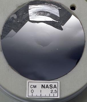
Pioneered by systems like the third-generation Cerebras Wafer-Scale Engine, wafer-scale integration transforms an entire 300-millimeter silicon disk into a single massive processor. Fabricated on a five-nanometer process node, the 46,225-square-millimeter chip houses four trillion transistors and 900,000 compute cores.
Rather than slicing the wafer into individual chips, foundry engineers deposit microscopic metal interconnects directly across the scribe lines that normally separate adjacent reticle exposure fields. Redundant routing paths and spare compute cores automatically bypass natural manufacturing defects on the silicon surface.
Keeping 44 gigabytes of static random-access memory distributed directly alongside compute cores delivers 21 petabytes per second of on-chip memory bandwidth. This breakthrough in semiconductor hardware technology enables massive language models to train and run inference without waiting on external memory buses.
Custom water-cooled cold plates and flexible printed circuit membranes absorb thermal expansion across the giant silicon slab while delivering 25 kilowatts of regulated power. Vertical current delivery eliminates the voltage drop that historically plagued early wafer-scale experiments in the 1980s.
Advanced 2.5D And 3D Chiplets Redefine Modular Scaling
In parallel, leading foundries and processor vendors have perfected 2.5D silicon interposers and 3D hybrid copper-to-copper bonding to assemble multi-die superchips. Instead of building every function on one costly silicon node, engineers pair high-density logic chiplets with stacks of high-bandwidth memory.
Chip-on-Wafer-on-Substrate packaging bridges adjacent reticle-sized logic dies using ultra-fine silicon wiring layers that match on-die bandwidth efficiencies. Vertical 3D stacking goes a step further by bonding cache memory directly atop processor cores through microscopic through-silicon vias.
Manufacturing smaller individual chiplets also reduces silicon wafer waste, since a single dust particle only ruins a tiny tile rather than an entire monolithic processor. Foundries are now expanding glass-substrate packaging lines to host dozens of interconnected tiles without warping under high heat.
Open die-to-die interface standards now allow chip architects to mix central processing cores, neural engines, and optical networking tiles from multiple fabrication nodes inside one package. By decoupling compute logic from memory controllers, wafer-scale engines and 3D chiplets ensure computing power scales long after monolithic Moore’s Law slows down.